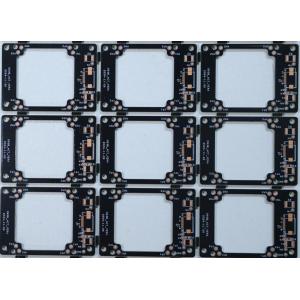
Black oil OSP double-sided board PCB is a double-sided printed circuit board that combines OSP (Organic Solderability Preservative) surface treatment with a black solder mask. It features a double-sided wiring design: the substrate (typically standard FR-4) is coated with black ink as the solder mask, which provides insulation, protects the circuit, and offers good light-shielding properties. Both sides of the board undergo OSP treatment on exposed copper surfaces, forming a thin organic protective film through chemical reactions to prevent copper oxidation while maintaining solderability. This PCB is suitable for small to medium complexity circuits and adapts to the welding needs of conventional and precision components in general operating environments.
Key Features of Double-sided PCB
- Dual-Sided Copper Cladding: Conductive copper foil on both top and bottom of the insulating substrate.
- Plated Through-Holes (PTHs): Enable electrical connection between the two copper layers for signal/current transmission.
- Balanced Performance-Cost: Higher component density and routing flexibility than single-sided PCBs, yet more cost-effective than multi-layer PCBs.
- Moderate Component Density: Supports more components (e.g., SMDs, through-hole parts) than single-sided PCBs, suitable for devices needing moderate functional integration without the complexity of multi-layer boards.
- Flexible Routing: Reduces wire crossing issues via two-layer routing, simplifying the layout of signal and power circuits for better performance.
- Wider Application Adaptability: Compatible with diverse electronic devices across consumer, industrial, automotive, and medical fields due to its balanced cost and functionality.
Common applications
● Telecom & Networking: Base stations, routers, and communication modules.
● Medical Devices: Portable instruments, monitors, and wearable tech.
● Industrial Control: PLCs, sensors, power modules, and automation systems.
● Consumer Electronics: Printers, home appliances, computers, and instruments.
● Automotive Electronics: ECU, lighting control, dashboards, and charging units.
● Aerospace & Defense: UAVs, communication terminals, and sensor boards.
● Emerging Tech: HDI designs for IoT, embedded systems, and high-density modules.
Main Advantages
- Reliable solderability: The OSP film is easily removed during soldering, enabling good solder wetting on copper surfaces, reducing cold solder joint risks, and ensuring stable connections even for fine-pitch components.
- Superior light-shielding and protection: The black solder mask provides effective light-shielding, preventing light interference in sensitive circuits; it also isolates circuits from external environments, enhancing corrosion and abrasion resistance.
- Cost-effectiveness: Combining the low-cost OSP process with economical black ink and standard substrates, the PCB has controllable production costs, suitable for cost-sensitive fields like consumer electronics and home appliances.
- Environmental friendliness: The OSP process uses non-toxic organic compounds, and the black ink is generally environmentally friendly, complying with environmental regulations and reducing hazardous waste.
- Dimensional precision: The thin OSP layer and black ink do not significantly affect the board’s thickness or flatness, making it suitable for high-density circuit designs requiring precise dimensions.