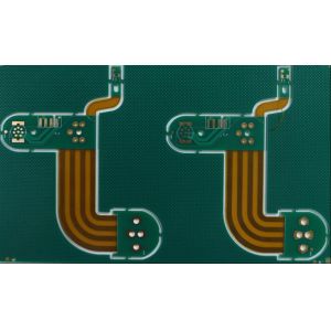
Industrial Control PCB Customized Board:
An industrial control board PCB (Printed Circuit Board) is a specialized circuit carrier that serves as the core "nerve center" for industrial control systems.
It integrates electronic components (like microchips, resistors, and capacitors) via printed copper traces, enabling stable signal transmission, precise data processing, and reliable control of industrial equipment. Unlike consumer-grade PCBs, it’s designed to withstand harsh industrial conditions—such as high/low temperatures, vibration, and electromagnetic interference—to ensure long-term, uninterrupted operation of devices like production line machines, process controllers, and power monitors.
Main Features:
- Focus on Harshness: Industrial PCBs prioritize survival and function under conditions (heat, cold, dust, moisture, vibration, electrical noise) that would quickly degrade consumer or commercial electronics.
- Reliability is Paramount: Every characteristic (materials, design, protection) aims for near-zero failure rates and continuous operation (24/7).
- Long-Term Perspective: Design and component sourcing ensure the board remains functional and supported for many years, often exceeding a decade.
- Industrial Ecosystem Integration: Built-in support for standard industrial interfaces and communication protocols is essential for connectivity.
- Certification & Compliance: Adherence to strict industrial safety and EMC standards is non-negotiable.
Industrial Control Board PCB Fabrication Process :
1. Design Data Transfer & DFM Check: The process begins with engineers submitting the Gerber files (design blueprints). The manufacturer conducts a Design for Manufacturability (DFM) check to ensure the design meets production tolerances.
2. Inner Layer Imaging & Etching: For multilayer boards, the circuit pattern is transferred onto the copper-clad laminate using a photoresist and UV light. Unwanted copper is then chemically etched away.
3. Lamination: The inner layers, insulating prepreg, and copper foil are stacked and bonded together under intense heat and pressure to form a solid board core.
4. Drilling & Plating (Vias): Precise drilling creates holes for component leads and vias (inter-layer connections). The hole walls are then plated with copper (electroless plating) to create electrical pathways between layers.
5. Outer Layer Imaging & Etching: The final circuit patterns are defined on the outer surfaces.
6. Solder Mask Application: A protective polymer layer (solder mask) is applied and cured, covering all traces except for the component pads.
7. Silkscreening: Component labels, logos, and reference designators are printed onto the board surface.
8. Surface Finish: A protective metallic finish (e.g., ENIG or HASL) is applied to the exposed copper pads to prevent oxidation and ensure solderability.
9. Electrical Testing & Profiling: The completed board is tested for opens and shorts (E-test). Finally, the large panel is cut (profiled) into individual PCBs.